The Planarization Process for Semiconductor Manufacturing
Planarization is a critical step in semiconductor manufacturing that involves creating a flat and smooth surface on a wafer. This process is essential for the successful fabrication of integrated circuits, ensuring uniform layer thickness and improved device performance. The planarization process is typically performed using chemical-mechanical polishing (CMP) or, in some cases, etching techniques. Here’s an overview of the planarization process using CMP:
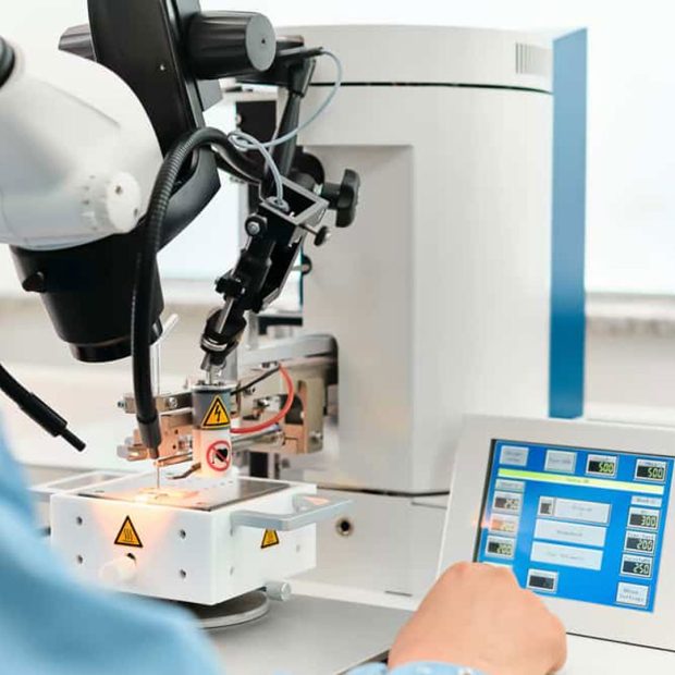
1. CMP Overview:
Chemical-Mechanical Polishing (CMP): CMP is the primary technique used for planarization in semiconductor manufacturing. It involves both chemical and mechanical actions to remove excess material and achieve a flat surface.
2. Substrate Preparation:
Before planarization, the semiconductor wafer undergoes various processing steps to create layers of materials, such as silicon dioxide, metals, or other dielectric and conductive materials.
3. CMP Components:
Polishing Pad: The CMP process occurs on a rotating polishing pad, typically made of a soft polyurethane material. The pad helps distribute the slurry and provides a controlled polishing environment.
Slurry: The slurry is a mixture of abrasive particles and chemical agents. It plays a crucial role in the removal of material during CMP.
4. Mechanical Action:
The wafer is pressed against the rotating polishing pad with controlled pressure. The mechanical action of the pad, combined with the abrasive particles in the slurry, removes material from the wafer surface.
5. Chemical Action:
Chemical agents in the slurry react with the material being polished. The chemical action helps in the removal of certain materials, providing selectivity and control over the planarization process.
6. Selectivity:
CMP is designed to be selective, meaning it removes specific materials while preserving others. For example, during the planarization of metal layers, the CMP process selectively removes metal material without significantly affecting underlying dielectric layers.
7. Endpoint Detection:
Endpoint detection is crucial to halt the CMP process when the desired layer thickness is achieved. Various methods, such as optical or acoustic monitoring, are employed to determine when the polishing should stop.
8. Post-CMP Cleaning:
After planarization, the wafer undergoes thorough cleaning to remove any residual slurry or particles. This ensures a clean and defect-free surface for subsequent processing steps.
9. Applications:
CMP is used for various applications, including planarization of interlayer dielectrics, metal layers, and shallow trench isolation. It helps in creating a smooth and flat surface for the deposition of subsequent layers and facilitates photolithography processes.
10. Advantages:
CMP provides excellent control over thickness uniformity and surface topography.
It allows for the planarization of different materials with high selectivity.
The process is highly repeatable and compatible with high-volume manufacturing.
11. Challenges:
Achieving uniform planarization across large wafer sizes can be challenging.
Selectivity and endpoint detection accuracy are critical for preventing over-polishing or under-polishing.
In summary, the planarization process, particularly using CMP, is a crucial step in semiconductor manufacturing to create flat and smooth surfaces, ensuring the success of subsequent fabrication steps and enhancing the performance of integrated circuits.